
A paper by the Erfu Liu Group and collaborators, “Excitonic Stark Response Induced by Quantum Capacitance in van der Waals Heterostructures,” has been published in Physical Review Letters. Xiangzhi Hong, a doctoral student at Nanjing University, is the first author, and Associate Professor Erfu Liu is the corresponding author. Congratulations to Xiangzhi Hong, Associate Professor Erfu Liu, and all coauthors.
How an applied voltage translates into an electric field inside a device depends on how electrons enter its constituent materials. The researchers found that graphene’s quantum capacitance alters interfacial charge transfer, causing the internal field to deviate from the conventional geometric model. They used two interlayer excitons with opposite dipole orientations as probes, extracting the residual electric field from their spectra and relating it quantitatively to graphene’s local chemical potential.

First, a test of electric-field cancellation
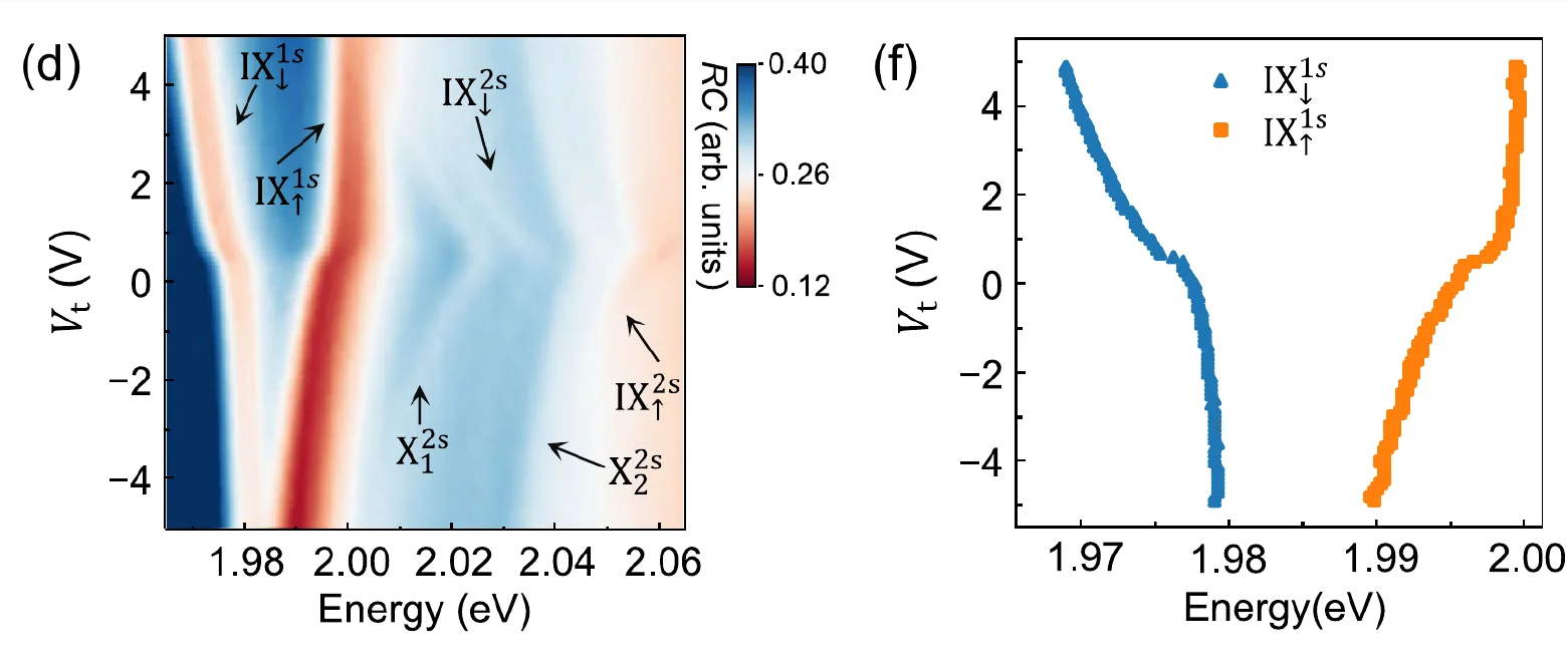
The top and bottom gates tune the charge density and electric field in the device. The team held the bottom-gate voltage fixed while varying the top-gate voltage, causing the gate-induced field and the field from transferred charge to change in opposite directions. The geometric capacitor model predicts equal and opposite changes, leaving the total field unchanged.

In measurements at approximately 6 K, however, the spectral lines of the two excitons still shifted, and by different amounts. This difference provided a clue to the residual electric field.
Separating the electric-field signal from the spectra
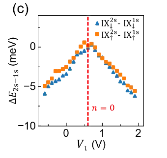
An interlayer exciton has its electron and hole distributed across adjacent atomic layers, giving it an electric dipole perpendicular to the layers. An electric field shifts the energies of excitons with opposite dipoles in opposite directions: the Stark response. The spectra also contain energy changes caused by carrier-dependent electronic interactions. By comparing the energy difference between the two branches, the researchers suppressed the approximately common many-body background and isolated the dipole-dependent response.

The team also compared the exciton ground and excited states. The 2s–1s spacings of the two dipole orientations changed nearly in unison with carrier concentration, indicating approximately symmetric binding-energy corrections. Together with an analysis of band-gap renormalization, this supports the conclusion that the main change in the energy difference comes from the residual Stark response.
From residual field to chemical potential
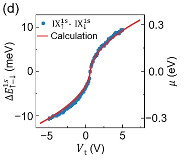
Graphene has a finite number of electronic states available in each energy interval. Changing its charge also changes its chemical potential; quantum capacitance describes the response of charge to that change. Geometric capacitance depends on device dimensions and dielectric properties, and both capacitances affect charge transfer. Quantum capacitance reduces the transferred charge relative to the purely geometric prediction, so the resulting field does not fully compensate the change in the gate field.

After quantum capacitance is included, the model agrees with the measured energy splitting without additional fitting parameters. In this configuration, the change in exciton splitting is proportional to the change in local chemical potential. With calibration, optical spectra can therefore be used to read out graphene’s local electronic state under an applied gate voltage.
These results show that quantum-capacitance corrections matter when interfacial charge transfer occurs and quantum capacitance is comparable to the relevant geometric capacitance. Differential spectroscopy of opposite-dipole excitons offers a micrometer-scale optical probe of local electronic properties at buried interfaces under operating conditions.
Professor Baigeng Wang contributed to the theoretical interpretation. Takashi Taniguchi and Kenji Watanabe at the National Institute for Materials Science provided the hexagonal boron nitride crystals used in device fabrication.
Paper: Physical Review Letters 137, 186902 (2026).
